Automated Optical Inspection (AOI) is another crucial non-destructive testing (NDT) method used in manufacturing and quality control. Unlike 3D X-ray testing, which uses X-rays to examine the internal structure of objects, AOI uses high-resolution cameras and computer algorithms to visually inspect the external surfaces of components and assemblies.
At Altest Corporation in San Jose, CA, AOI testing would likely be employed for inspecting the external quality of various products, especially in industries like electronics, automotive, and medical devices. Here’s how AOI works, its applications, and how it could be utilized by Altest Corporation.
Automated Optical Inspection involves the following key steps:
High-resolution cameras (often using visible light or sometimes infrared light) capture detailed images of the surface of an object, typically a printed circuit board (PCB) or a component.
These images are processed by sophisticated software algorithms that can analyze the captured images in real time. The software compares the actual appearance of the object to pre-defined models or specifications (CAD files, design rules, or standards).
The system looks for discrepancies, such as:
Based on the analysis, the system provides a pass or fail result, and can also flag areas for further manual inspection if needed.
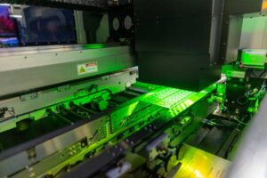
AOI is widely used in industries where precision and reliability are critical, particularly in:
AOI is especially useful in PCB assembly for detecting soldering defects, incorrectly placed components, missing components, or broken connections.
AOI systems can inspect components like wiring harnesses, LED assemblies, and mechanical parts to ensure that they are defect-free before assembly.
Medical device manufacturers use AOI to ensure that the surface finishes, component placements, and assembly integrity of devices like catheters, implants, or surgical instruments meet stringent quality standards.
AOI can be used to ensure that products like batteries, small mechanical devices, or consumer electronics are free from manufacturing defects.
AOI is much faster than manual inspection, allowing for real-time feedback and quicker detection of defects, which is critical in high-volume manufacturing environments.
The automated nature of AOI ensures that inspections are consistent across the entire production run, reducing human error and variability.
AOI systems can detect minute defects with incredible accuracy, including very small soldering issues, surface imperfections, or minor misalignments that would be hard for the human eye to detect.
While AOI systems may require an initial investment in equipment, they can significantly reduce labor costs associated with manual inspection, and they can operate 24/7 without fatigue.
AOI is entirely non-destructive, meaning the components or assemblies being tested can be re-used or moved to the next stage of production without any damage.
At Altest Corporation in San Jose, CA, AOI testing would likely be a critical part of their quality assurance and failure analysis services. Their services could include:
Altest may use AOI to inspect products in high-volume production lines, ensuring that any defects are caught early in the process. This helps to prevent faulty components from moving forward to later stages of production or reaching customers.
For customers who are in the prototype development phase, Altest can use AOI to help quickly identify design flaws or manufacturing issues, ensuring that products meet the necessary specifications before mass production.
In electronics, solder joint inspection is a primary application of AOI. Altest may employ AOI systems to examine solder joints for cold soldering, solder bridges, insufficient solder, or incorrect component placement.
Altest’s AOI solutions can automate the visual inspection process, allowing them to deliver high-throughput, error-free quality checks for customers in industries like electronics, automotive, and medical devices.
Captures a flat image of the object and analyzes it. It’s typically used for detecting surface defects or component misplacement.
Uses advanced technologies such as laser triangulation or stereo vision to capture the height profile of a component, enabling detection of soldering defects (such as solder bridges or insufficient solder) and component height issues.
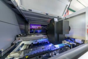
By identifying defects early in the process, AOI can help prevent delays caused by defective products being caught late in the manufacturing process.
With AOI, customers can ensure the quality of their products by detecting defects early, leading to improved overall product reliability and customer satisfaction.
Detecting defects in real-time minimizes the need to scrap entire batches of products, saving money and resources in the long run.
Frequently Asked Questions About AOI Testing
Automated Optical Inspection (AOI) testing is a non-destructive inspection method that uses high-resolution cameras, lighting, and computer software algorithms to visually inspect components and assemblies. In PCB manufacturing, AOI testing is used to identify defects such as missing components, component misalignment, soldering defects, incorrect component placement, and orientation errors.
AOI testing works by capturing high-resolution images of a PCB or component using cameras and analyzing those images with specialized software. The system compares the actual appearance of the PCB with predefined models, CAD files, design rules, or specifications to identify potential defects. The AOI system then provides a pass or fail result and can flag areas that require further inspection.
AOI testing can detect a wide range of PCB defects, including component misalignment, missing components, incorrect component placement, soldering defects, solder bridges, cold solder joints, insufficient solder, package orientation errors, broken connections, scratches, and other surface imperfections.
AOI testing is important for PCB assembly because it helps identify manufacturing defects early in the production process. Automated inspection provides consistent and accurate quality checks, helping manufacturers prevent defective PCBs from moving to later production stages and improving overall PCB quality and reliability.
2D AOI captures a flat image of the PCB or component and analyzes it to identify surface defects, component placement problems, and other visual issues. 3D AOI uses technologies such as laser triangulation or stereo vision to capture the height profile of components, providing additional information for detecting soldering defects, solder bridges, insufficient solder, and component height issues.
Yes. AOI testing can detect various soldering defects during PCB assembly. These may include cold solder joints, solder bridges, insufficient solder, and other solder-related issues. AOI systems inspect solder joints visually and compare them against predefined specifications.
Automated Optical Inspection can detect defects including missing components, incorrectly placed components, component misalignment, incorrect component orientation, solder bridges, cold solder joints, insufficient solder, broken connections, scratches, and other surface or assembly defects.
AOI testing services are used across industries where precision, reliability, and quality control are important. These include electronics and PCB manufacturing, automotive, medical devices, consumer electronics, and other manufacturing applications where components and assemblies require accurate inspection.
Yes. AOI testing is a non-destructive testing method. The inspection process does not damage the components or assemblies being tested, allowing products that pass inspection to be reused or moved to the next stage of production.
AOI testing provides several benefits for PCB manufacturing, including faster inspection, consistent quality control, high inspection accuracy, reduced human error, early defect detection, and reduced labor requirements. AOI systems can also opera
Rigid Board Assembly refers to the process of assembling electronic components onto a rigid PCB (Printed Circuit Board), which is a non-flexible, solid substrate used to support and electrically connect components such as resistors, capacitors, integrated circuits (ICs), and connectors. Unlike flexible or rigid-flex boards, rigid PCBs maintain their shape and are typically used in a wide range of electronic devices and applications, from consumer electronics to industrial equipment.
The assembly of rigid PCBs is a multi-step process involving several key stages, including design, fabrication, component placement, soldering, and testing.
Before the assembly process begins, the PCB design must be finalized. This step is essential for creating a functional and manufacturable rigid board.
The BOM specifies the components to be used, including resistors, capacitors, ICs, and connectors, and is used for sourcing parts.
After the design is finalized, fabrication files are generated (such as Gerber files and NC drill files) for the PCB manufacturer to produce the rigid PCB.
The PCB fabrication process creates the physical rigid board according to the design files. The key steps in this process include:
Rigid PCBs are typically made from fiberglass (such as FR4), which is a durable, non-flexible material that provides mechanical strength and electrical insulation.
Other materials like CEM-1 or CEM-3 are sometimes used for specific applications.
For multi-layer boards, the process involves stacking several layers of conductive and insulating materials, which are then laminated together using heat and pressure.
The inner layers of the PCB (for multi-layer designs) are often created by etching copper onto a substrate and then bonding them with additional layers.
A thin layer of copper foil is laminated onto the board, and then the unwanted copper is removed via an etching process. This creates the conductive traces that will carry the electrical signals.
The surface of the PCB is treated with a finish to protect the copper and improve solderability. Common finishes include HASL (Hot Air Solder Leveling), ENIG (Electroless Nickel Immersion Gold), or OSP (Organic Solderability Preservative).
After the PCB is fabricated, the next step is to source the components and place them onto the board. This process typically includes:
Soldering is the process that permanently attaches the components to the PCB by forming electrical connections through melted solder. The main soldering methods used in rigid board assembly include:
In cases where automatic methods are not feasible or for small production runs, hand soldering with a soldering iron may be used, particularly for small or delicate components.
Once soldering is complete, it’s critical to ensure that the PCB assembly is functional and free from defects. This involves several stages of inspection and testing:
ICT tests the functionality of the individual components and checks for shorts, opens, and other faults. It involves applying test signals to the circuit and verifying that the outputs match the expected results.
After ICT, functional testing is performed to verify that the entire PCB assembly works as intended in the real-world application. This may involve testing the board with power applied and running through its intended use cases.
For boards with fine-pitch components (e.g., BGAs) or multi-layer structures, X-ray inspection can be used to check the internal solder joints and vias for defects that are not visible on the surface.
After testing and inspection, the PCB is cleaned to remove any flux residues, soldering debris, or other contaminants that could affect performance or longevity.
Before the assembled PCBs are shipped to the customer or integrated into the final product, they undergo a final inspection to ensure they meet quality standards.
Rigid PCBs are widely used across many industries and applications, including:
In the world of modern electronics and product development, ensuring the reliability and functionality of complex systems is crucial. One of the most effective strategies for achieving this is through Design for Testability (DFT) engineering. DFT focuses on designing products in a way that makes them easier to test during and after manufacturing, ensuring that any faults or defects can be quickly identified and rectified. This approach is especially important in industries such as electronics, automotive, aerospace, and telecommunications, where product failure can lead to significant costs, safety risks, and reputational damage. This article will explore what DFT engineering is, its importance, principles, and how it is applied in modern manufacturing.
Design for Testability (DFT) is an engineering practice that integrates testability into the design phase of product development. The goal of DFT is to ensure that a product is designed in a way that allows for easy and efficient testing of its functionality, performance, and reliability throughout its lifecycle. DFT aims to create systems that are not only functional but also easy to diagnose, troubleshoot, and validate during production and after deployment.
DFT is particularly critical in industries where products are complex, have multiple components, and are expected to function in challenging environments. By addressing testing early in the design process, DFT helps ensure that products meet high standards of quality, reliability, and safety.
Implementing DFT engineering principles offers several significant benefits to manufacturers and product developers, including:
Several core principles guide DFT engineering practices. These principles focus on improving the ease and effectiveness of testing throughout the product lifecycle:
DFT principles are applied in various industries to enhance product performance, ensure reliability, and reduce testing costs. Let’s take a closer look at how DFT is implemented in different sectors:

