Design for Test (DFT) is a hardware engineering methodology that integrates testing features directly into an integrated circuit (IC) or system-on-chip (SoC) during the design phase.
Controllability: The ability to set specific logic states (0 or 1) at any internal node in the circuit using primary inputs.
Engineers implement several structural techniques to automate testing using Automatic Test Equipment (ATE).

DFT Design For Test Modifies sequential circuits (like flip-flops) by linking them into long shift registers called "scan chains." This allows test patterns to be shifted in serially, applied to combinational logic, and shifted out for analysis.
Built-In Self-Test (BIST): Embeds autonomous test circuitry directly on the chip. It includes a Test Pattern Generator (TPG) to apply stimuli and an Output Response Analyzer (ORA) to check the results. It is widely used for embedded memories (MBIST) and logic (Logic BIST).
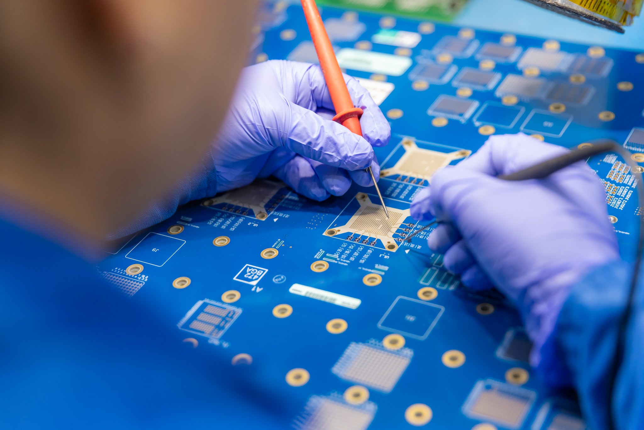
Our engineers prepare PCB layouts specifically for automated in-circuit testing by ensuring adequate spacing, accessibility, and probe compatibility.
Flying Probe Test Optimization:Ideal for prototypes and low-volume production, we optimize PCB layouts for flying probe testing without requiring expensive fixtures.
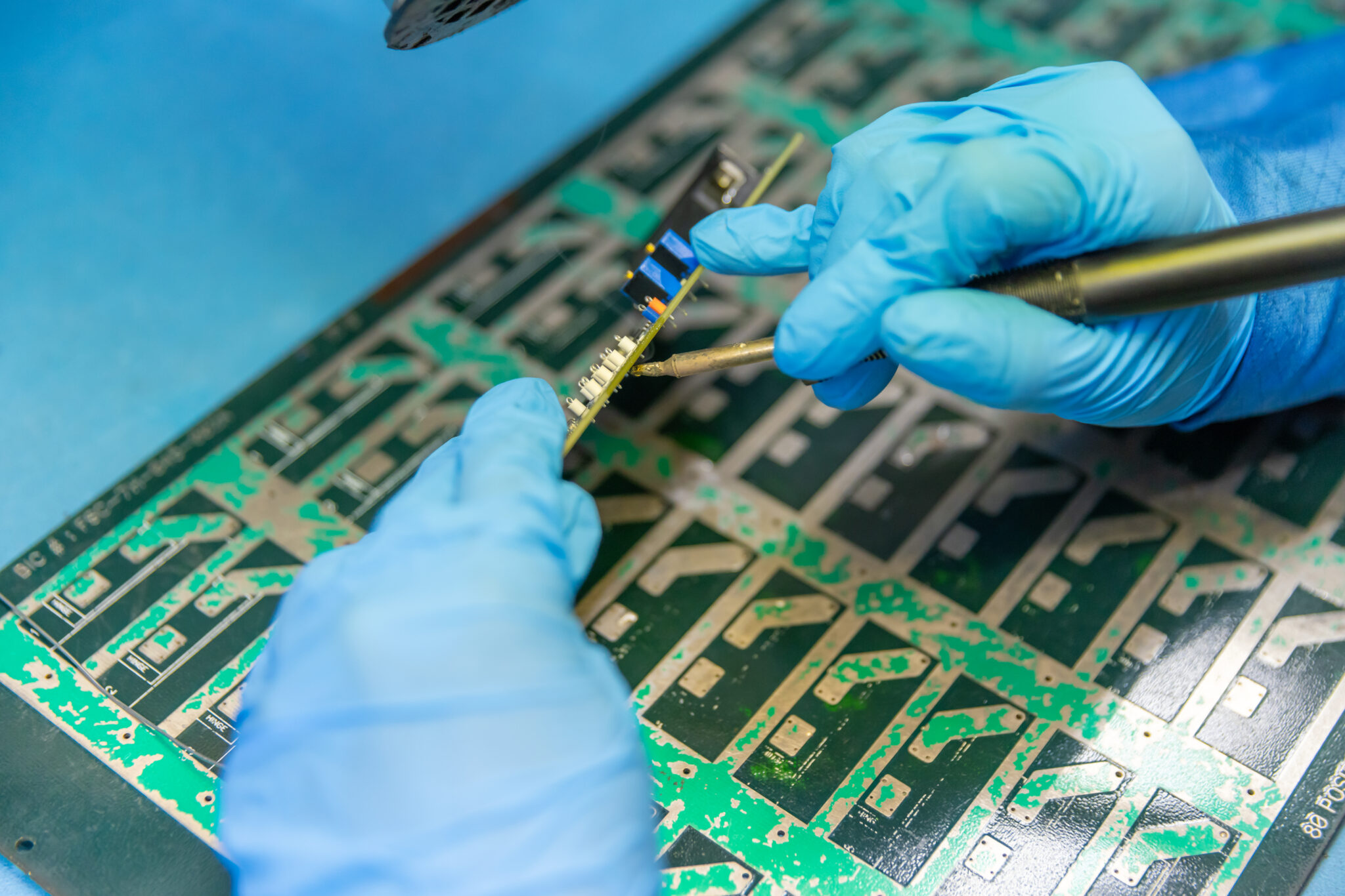
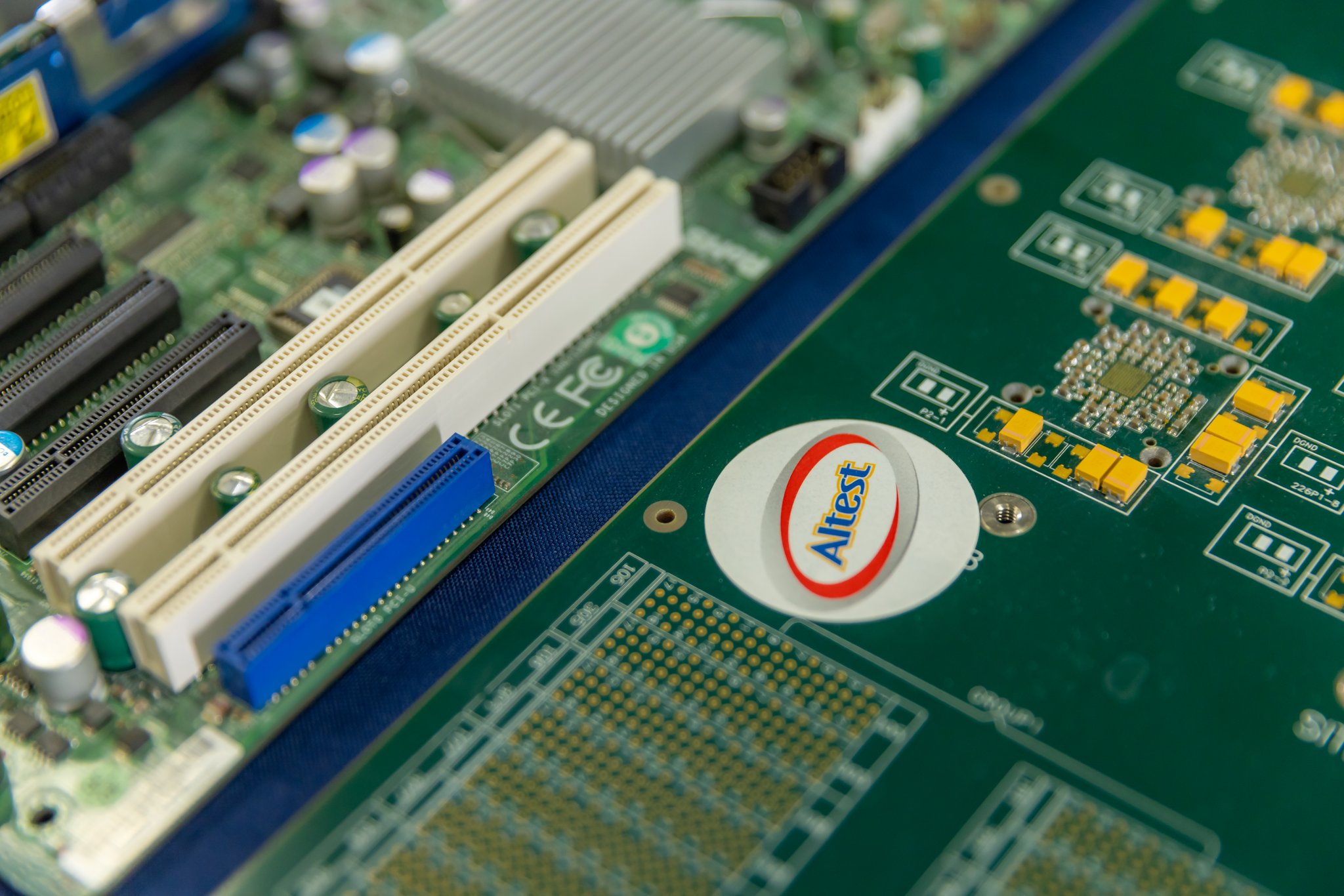
Functional Test: We design boards that simplify end-of-line functional testing, ensuring all major electrical functions can be validated quickly and accurately.
Boundary Scan (JTAG):For high-density PCBs and complex digital systems, we implement JTAG-compatible design practices to simplify testing of inaccessible circuits.
Debug & Diagnostics Optimization:We improve board accessibility for engineers during prototype validation and failure analysis.
Find answers to common questions about test point accessibility, test coverage optimization, Boundary Scan (JTAG), and ensuring post-assembly reliability.
DFT is the engineering practice of designing a printed circuit board with specific features—like dedicated test points and accessible electrical nodes—that make it easier, faster, and more comprehensive to test the board for manufacturing defects after it is assembled.
While a design may work perfectly in software, physical manufacturing is never flawless. Components can be placed backwards, solder can bridge across pads, or a trace might be severed. DFT ensures that when the physical board is built, automated testing machines can quickly pinpoint exact assembly defects without requiring slow, manual troubleshooting.
DFM (Design for Manufacturing) focuses on ensuring the board can be physically built efficiently and reliably (e.g., proper trace spacing, avoiding acid traps). DFT (Design for Testing) focuses exclusively on ensuring the board can be thoroughly electrically inspected after it is built. Both are critical for high-yield, cost-effective production.
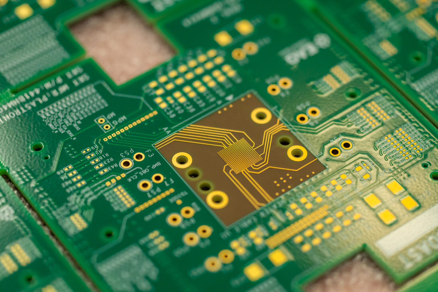
Test points are small, exposed areas of copper (often circular pads) intentionally placed on the PCB surface. During the DFT layout phase, our engineers strategically route these points to critical electrical nets so that automated testing probes can physically touch them to measure voltage, current, and component values.
Proper DFT implementation requires minimal space and adds virtually zero cost to bare board fabrication. In fact, by drastically reducing the time it takes to run the final assembly through Flying Probe or ICT machines, and by eliminating manual troubleshooting, DFT significantly lowers your overall production and labor costs.
A thorough DFT layout optimizes the board for a suite of automated inspection methods, primarily Flying Probe Testing (FPT) for prototypes and low-volume runs, In-Circuit Testing (ICT) via custom bed-of-nails fixtures for high-volume production, and Boundary Scan testing.
Yes, but it requires advanced engineering. Adding physical test points to high-speed digital or RF traces can create "stubs" that act as tiny antennas, causing signal reflection and impedance mismatch. We use specialized techniques like boundary scan integration or strategic probe placement on non-critical low-speed nodes to ensure testability without compromising signal integrity.
Boundary Scan, often utilizing the JTAG (IEEE 1149.1) protocol, is a sophisticated DFT technique used to test interconnects between complex digital chips (like microprocessors, FPGAs, and memory). It uses the internal silicon logic of the components to verify that the pins are soldered correctly, which is vital for testing densely packed boards and fine-pitch BGAs where physical probes cannot reach.
DFT must be implemented as early as possible, ideally during the schematic capture and initial component placement phases. Trying to retrofit test points onto a fully routed, densely packed multi-layer board is incredibly difficult, time-consuming, and often requires costly layout compromises.
Our goal during a DFT review is to maximize your structural fault coverage. We aim to ensure that the vast majority of critical nets and components on the board are accessible by our testing equipment. High test coverage guarantees that any manufacturing defect will be caught and corrected before the product ever ships to your end customer.
Partner with Altest Corporation for your next high-reliability PCB fabrication and turnkey SMT assembly project. Our engineering team is ready to review your gerber files and provide a detailed, competitive estimate.

