PCB Fabrication
PCB fabrication is the process or procedure that transforms a circuit board design into a physical structure based upon the specifications
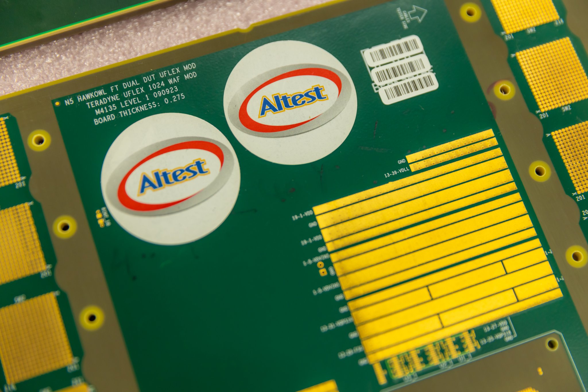
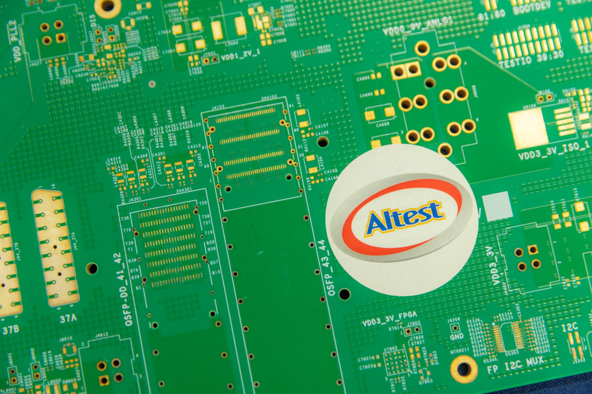
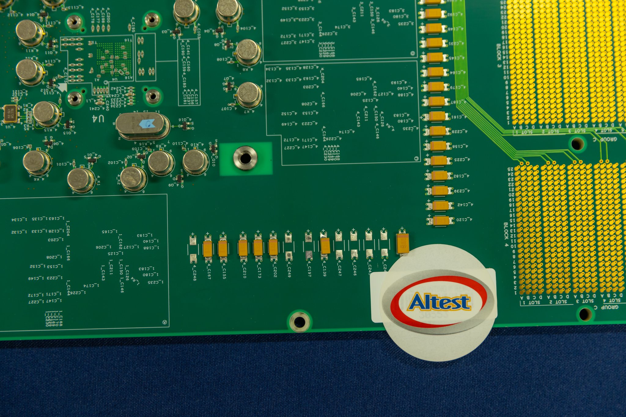
What is PCB Fabrication
✔PCB fabrication : PCB fabrication is short for printed circuit board fabrication, it is the complete manufacturing process of realising a design with circuit patterns into a physical and functional PCB bare board.
✔PCB Type: Rigid, Flex, Rigid-flex, Semi-flex, HDI, RF & microwave, IC Substrate
✔PCB Materials: FR4, Polyimide, Kapton, PET, Aluminum-based, Copper-based, Metal-based, Alumina Ceramic, Ceramic, Hybrid material, Halogen free, High Speed, High frequency, PTFE, Teflon
✔Layers: Multilayer up to 60+ layers,
-
Common Types of PCB Fabrication
The classification of PCB boards is hard to define. However, the most common is number of layers and substrate used. (1) number of layers: single-sided PCB, double-sided PCB and multi-layer PCB; (2) substrate used: rigid PCB, flexible PCB, and rigid-flexible PCB.
-
Single-sided PCB
Single-sided PCB is the least cost and simplest PCB type made with one layer of copper on one side. Electrical components are also populated on one side only. The low cost is due to simple PCB fabrication services and few components.
-
Double-sided PCB
A double-sided PCB is a kind of circuit board with two copper layers, which are the top copper layer and the bottom copper layer. The top copper layer and bottom copper layers are connected by through-holes.
-
Multi-layer PCB
a multi-layer PCB consists of several working layers, with the top layer acting as the surface for component placement while the bottom layer for routing and welding.
Industries We Serve:
Main Steps in PCB Fabrication
Circuit Design
A circuit design must first be generated using a Computer-Aided Design (CAD) software system. The design workflow starts with circuit development, layout definition and CAD program generation.
Patterning
The patterning process can be done through ‘photolithography’. In photolithography, a photosensitive material, also known as photoresist, is coated into the copper foil and then exposed to light.
Drilling
Recall that vias are the structures that connect layers. This is made possible by drilling a hole using mechanical or laser drill. The drilling process is usually the bottleneck of PCB fabrication service.
Via Filling
The inner walls of the vias should be plated with copper, which is a conductive material enabling the vertical structures to electrically connect different layers. PCB fabricators can choose from electrolytic to electroless plating methods.
Solder Mask
As briefly discussed earlier, a solder mask is a thin protective polymeric layer that is deposited into the FR-4 laminate to help isolate the conductive and insulating surfaces. The solder mask layer can be achieved through several direct and indirect deposition techniques
Surface Finishes
The exposed copper trace on the copper pads of the fabricated PCBs is protected from external environment through surface finish like HASL, OSP, ENIG, ENEPIG, immersion gold, immersion silver, immersion tin., etc.
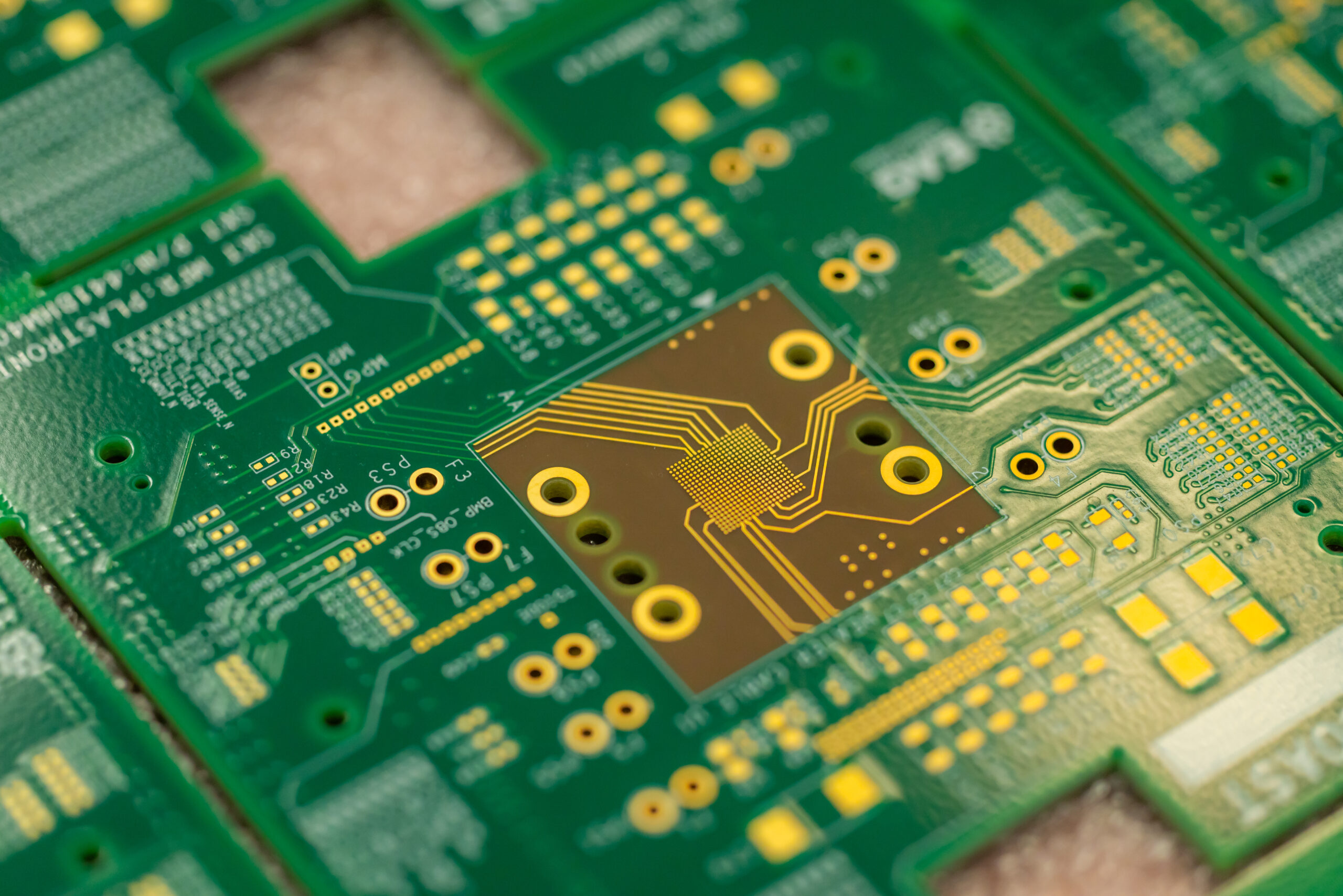
Basic Materials in PCB Fabrication
-
Dielectric Material
- Solder Mask
- Core
- Copper Foil
- Vias
The material that is sandwiched between the copper layers is known as dielectric material. This material can further be divided into core and prepreg. As mentioned earlier, the most commonly used dielectric material is FR4 which means resin impregnated woven glass fabric. Most PCB fabricators use FR-4 as a default substrate material.
The solder mask primarily serves as protection of the copper layer from corrosion due to exposure to outside environment. The solder mask also guides the solder along the copper pad.
A core consists of two copper foil sheets with an insulating layer in between. The copper is used for conductivity while the insulating layer is used for mechanical support and electrical insulation.
Copper traces and pads are drawn on each layer using a layout tool, but the PCB fabricator actually starts with a complete layer of copper. The copper that is not required in the design is being etched away. The copper pads that are being used for surface mounting still require a surface finish as copper is now easily oxidized.
As reiterated in the prior sections, the layers are insulated from each other, thus a structure is needed to allow the layers to connect. This is realized by drilling a copper plated hole, allowing connection from one layer to another. There are also various types of vias that depend upon the design and complexity of the device:
- Through-hole: The most popular and cheapest method where the vias connect one layer to another.
- Blind: Vias connect the top or bottom to the internal layer but does not go through all the layers.
- Buried: This via does not extend to the top or bottom layer, because it connects only the internal layers.
- Micro via: Very small vias that are drilled through laser, mostly used for small pitch and high-density devices.
The cost of fabricating PCB highly relies on the number of vias due to the additional steps required like drilling and copper plating.
Our Certifications