Altest PCB Testing
Altest entire spectrum of testing equipment ensure complete functionality and deliverability of your PCB design.
At every stage of production, we run a series of checks to ensure that you have an end-to-end hassle-free experience.

AOI (Automated Optical Inspection)
- AOI (XL / 3D) provides the quick and precise inspection required to ensure that the product is of high quality without any manufacturing defects.
- 3D Inspection
- Board Size: 850mm x 610mm (33.46” x 24”)
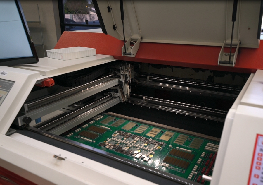
Flying Probe
- Flying Probe Test is an electrical PCBA test.
- Flying Probe Test Requirements
- Visual Tests for component presence, absence, and rotation
- CAD data: ODB++(Ver 7), IPC356, or Allegro ASCCI file
- Test ICs for open tracks on the PCBA
- Schematic file for troubleshooting the PCBA
- Isolation Test to detect shorts on the PCBA
- Standard analog in-circuit test
3D X-Ray
- The 3D X-Ray tool enables us to inspect components that may not be visually accessible from the top and/or bottom.
- Detect Solder Bridge’s, Cold Solder and Voids
Functional Test
- Continuity Test
- AC/DC Voltage Test (Input and Output)
- Electrical Test to duplicate or reproduce the incorrect operation of the component.
