Design For Test (DFT)
Design For Test (DFT) is an engineering practice that integrates testability into the design phase of product development.
Design For Test
- Reduced Testing Costs: By designing products for ease of testing, manufacturers can reduce the time, labor, and equipment costs associated with testing. DFT allows for the automation of testing processes, enabling faster and more accurate testing.
- Improved Product Quality: DFT helps identify potential issues early in the design process, reducing the likelihood of defects in the final product. It ensures that test coverage is comprehensive, leading to higher-quality products that meet customer expectations.
- Faster Time-to-Market: Effective DFT practices can streamline the testing process, allowing companies to identify and resolve issues more quickly. This accelerates the product development timeline, enabling companies to bring products to market faster.
- Enhanced Reliability and Safety: DFT ensures that products undergo thorough testing, which helps identify and address potential failure points before they can compromise the product’s performance or safety.
- Easier Maintenance and Repair: Products designed with testability in mind are easier to maintain and repair in the field. This improves product longevity and customer satisfaction, as issues can be quickly diagnosed and corrected.
Industries We Serve:
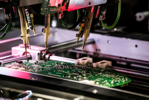
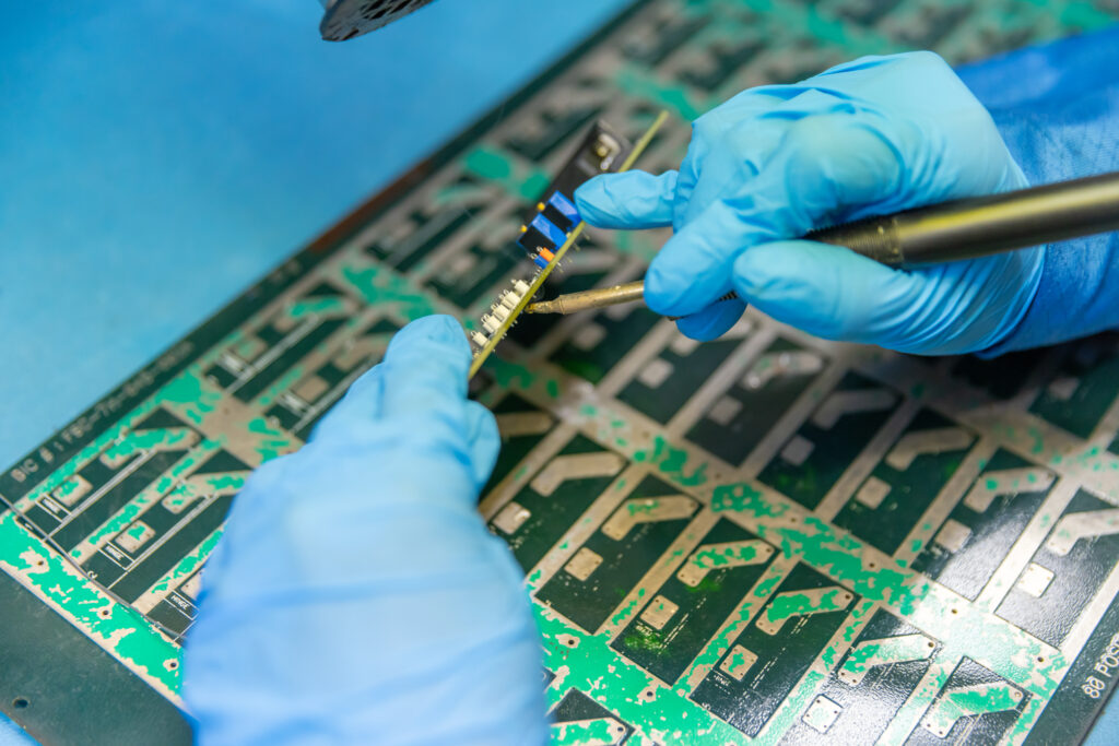
How It Works
Circuit layers
The PCB stack-up design clearly defines each and every layer and its order, there should be physical labels on each layer for their accurate placement.
Soldermask and Solderpaste
solder mask is the material applied to the circuit board to protect it and paste mask is the pattern used to apply the solder paste
Drill files
NC Drill File is also known as numeric control drill file. This indicates a file that regulates all the information relating to via or hole drilling requirements.
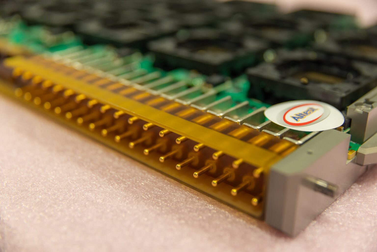
Plated and NonPlated Through-holes
The plating on the through holes is copper, a conductor, so it allows electrical conductivity to travel through the board. Non-plated through holes do not have conductivity,
Per-layer Blind
Blind vias are essential for multilayer PCBs, allowing efficient and reliable connections between the various layers without resorting to traditional through-hole vias that span the entire board.
BOM
A PCB bill of materials (BOM) is a comprehensive list that provides information on all the components to be assembled on your board.
PCB Reverse engineering Advantages
- Mission
- Vision
- Philosophy
Our Certifications