is creating a schematic diagram or circuit diagram that outlines the electrical connections between components in an electronic system.
Schematic Capture
Selecting Components: Choosing the right electronic components, such as resistors, capacitors, transistors, and integrated circuits (ICs), based on the design requirements.
Component Placement: Arranging the components logically in the schematic editor, ensuring proper flow of signals and power across the system.
Wiring Connections: Drawing the electrical connections (often represented as lines or traces) between the components to represent how they communicate and interact within the circuit.
Simulation and Verification: Using simulation tools to verify that the design works as expected before it is turned into a physical circuit. This step ensures that there are no errors or conflicts in the schematic
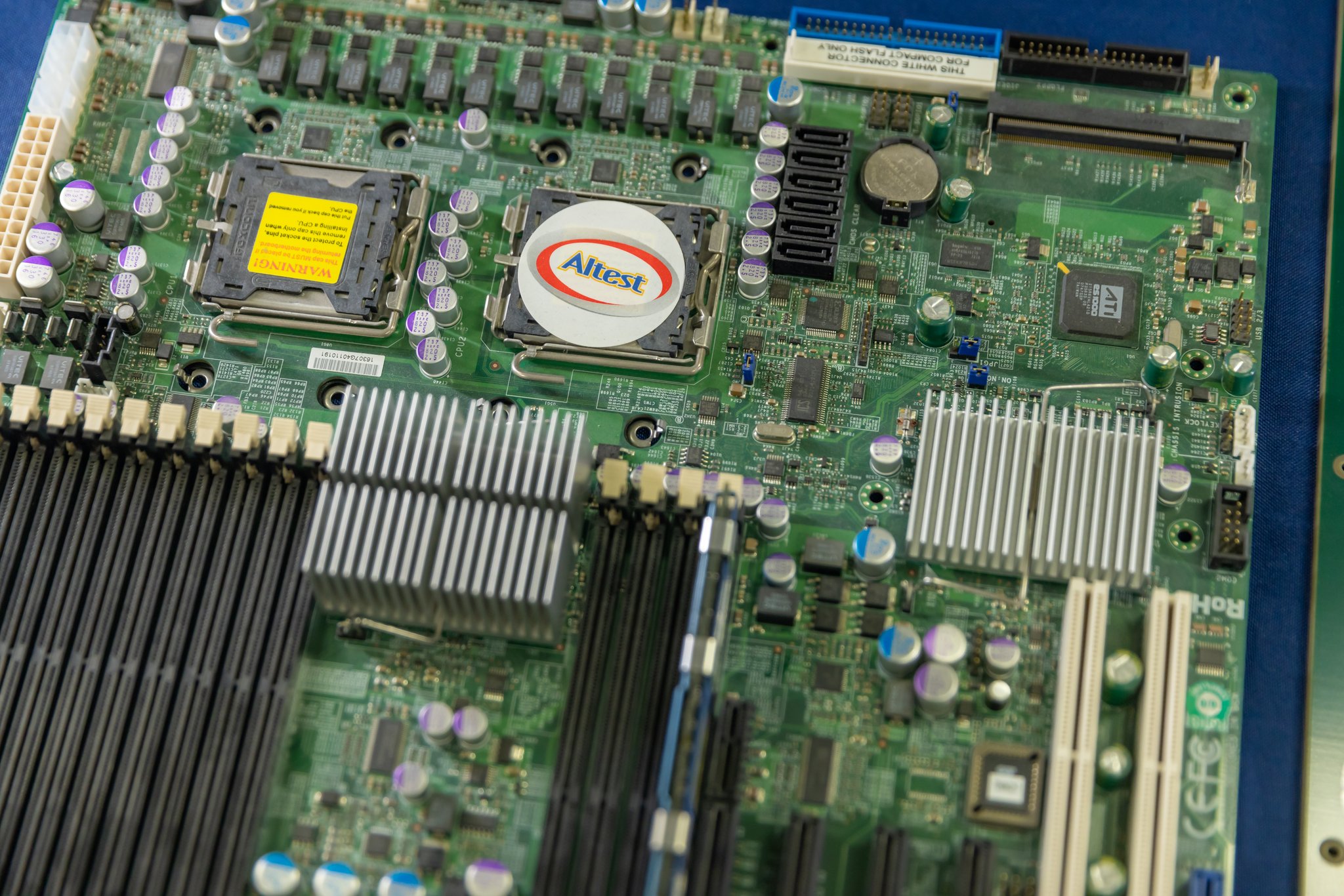
The PCB stack-up design clearly defines each and every layer and its order, there should be physical labels on each layer for their accurate placement.
Soldermask and Solderpaste
solder mask is the material applied to the circuit board to protect it and paste mask is the pattern used to apply the solder paste
Drill files
NC Drill File is also known as numeric control drill file. This indicates a file that regulates all the information relating to via or hole drilling requirements.
Plated and NonPlated Through-holes
The plating on the through holes is copper, a conductor, so it allows electrical conductivity to travel through the board. Non-plated through holes do not have conductivity,
Per-layer Blind
Blind vias are essential for multilayer PCBs, allowing efficient and reliable connections between the various layers without resorting to traditional through-hole vias that span the entire board.
BOM
A PCB bill of materials (BOM) is a comprehensive list that provides information on all the components to be assembled on your board.