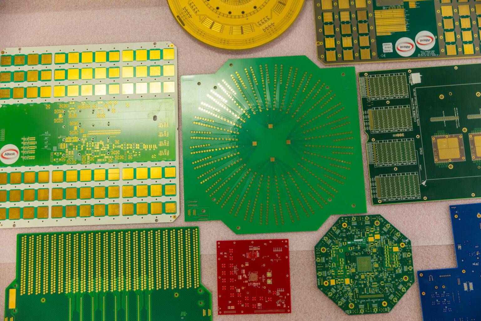
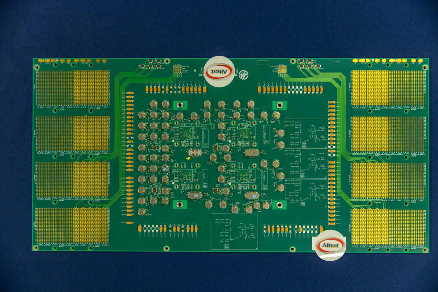
HDI- High Density Interconnect PCBs
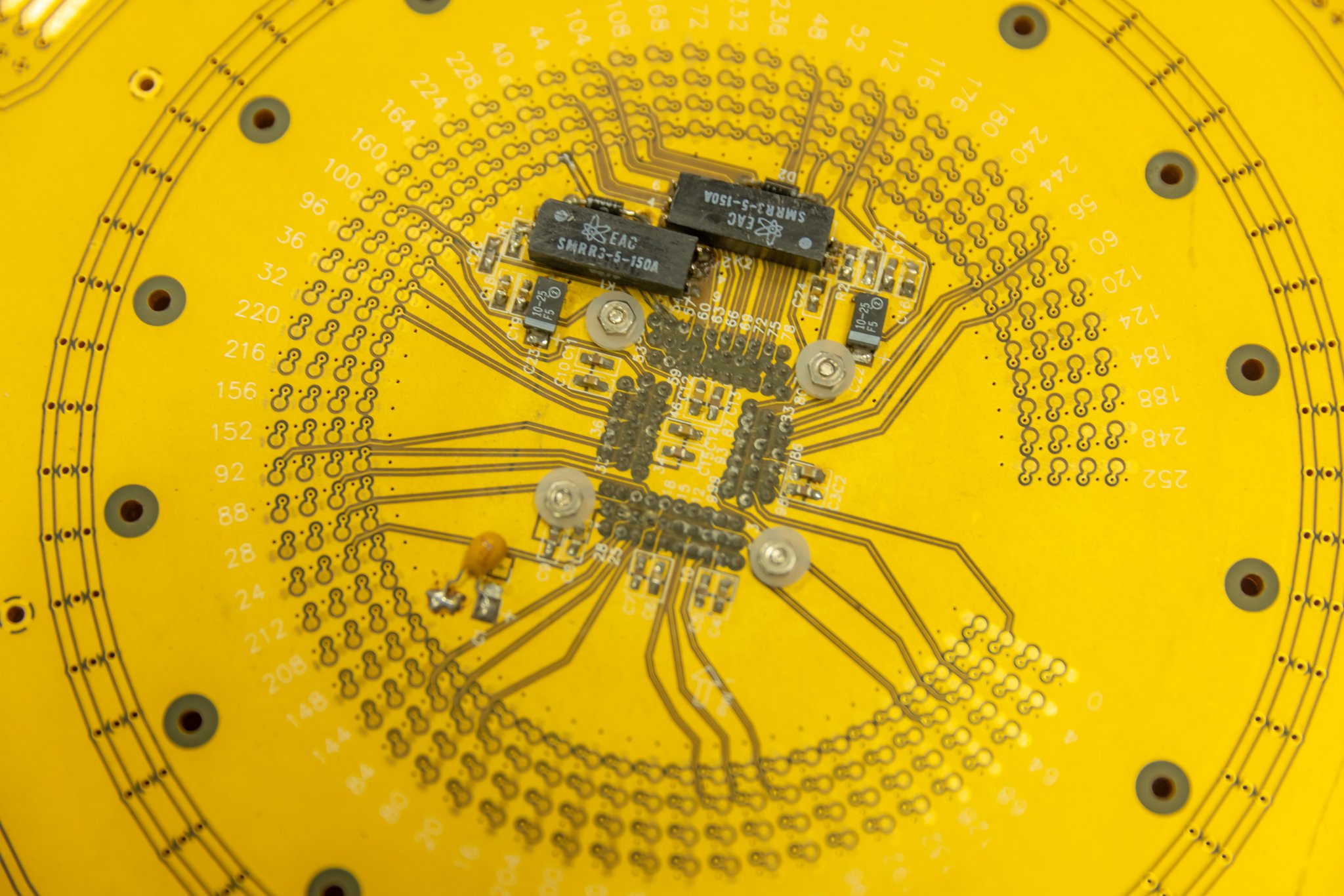
The full name of HDI PCB is high-density interconnect printed circuit board. It means the PCB has smaller traces, drills and more components packed in that space. Traces connecting the components and ICs are very thin and the current carrying is also very low.
Main featuers of HDI PCB ?
✔ Higher Layer Count :
Since HDI circuit boards are usually designed with very complex functions within our compact PCB area, so many traces and connections need to be spread into several layers. Usually, a HDI circuit board should have 4 layers at least, and most of the high density interconnect PCBs range Up to 12L “any layer” stacked uVia Structure
✔ Small Trace Width and Spacing
As a lot of traces need to be routed in a small space, it is obvious that the trace width and spacing need to be designed as small as possible. So most of the high density interconnect PCBs have trace width and spacing as small as 4 mil or below. In some designs, the trace width and spacing are 2mil which is very difficult in PCB production.
✔ Used Micro Vias
HDI circuit boards require smaller vias where the drill hole is less than 6 mils, therefore the vias need to be stacked with micro vias in between the layers. Micro vias are generally filled or plated in standard practice. High-density Interconnect PCBs require more area for routing so via in pad (VIP) technology is used to increase the density.
What are Advantages of HDI Printed Circuit Board
✔ Size and Weight: Compact size and light weight are the major advantages because of the footprint design and complexity of the board which retains the functional features in the overall big picture.
✔ Low Cost: The cost of manufacturing may seem high but when the entire standard PCB design is considered with components and size, this reduces the cost by multiple times in the overall application.
✔ Performance & Reliability: The performance of HDI circuit board is higher with reduced noise and signal integrity issues. Though the component package is small and the spacing is also small the HDI performs with reliability.
✔ Time to Market: The production process of high-density interconnect PCB shows excellent performances with less time for production and testing compact applications
Industries We Serve:
Why Choose HDI High-density Interconnect PCBs
Highest Industrial Quality Standards
Our PCBs are engineered for optimal performance, ensuring minimal signal loss and maximum reliability. Benefit from precise impedance control and stable signal integrity, crucial for high-frequency applications.
Customized Solutions
We understand that every project is unique. Our team works closely with you to deliver customized PCB solutions, meeting specific design requirements and industry standards.
Rapid Prototyping & Production
Speed up your development cycle with our rapid prototyping services. Quickly move from design to production while maintaining high-quality standards.
Altest’s Corporation HDI PCB Manufacturer
-
Quality Standards
- Advanced Equipment and Technology
- One-Stop Services
Our Certifications