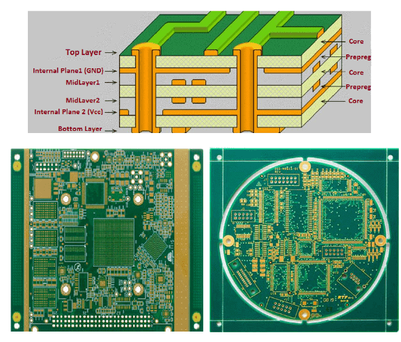
Multilayer PCB
A multilayer PCB is a printed circuit board with more than two copper layers. By contrast to single and double-layer PCBs which only have one or two copper layers. The multilayer printed circuit board range is 4 to 18 layers normally and even goes up to 100 layers in special applications
Manufacturing Process of Multilayer PCB
DFM Check : In this verification check, all layers are verified by the DFM engineer. He verifies all types of errors in the PCB. So, it would be easy for the production floor to make boards without any errors
Inner Layers Process:At this stage, the inner layer image was transferred to the printed circuit board using UV films and dry films, and then etching was done.
AOI (Automated optical inspection): AOI means automated optical inspection. So, this inspection converts the circuitry image to digital images. Also, AOI inspects the board to ensure it is free from defects. Then the manual visual inspector verifies the inner layers manually
Lamination:Lamination is the process of combining or bonding the inner copper foil, core, and prepregs to make solid layers. Lamination machines are set up with some parameters to heat and pressure those inner layers to make a solid layer
Drilling: Multilayer printed circuit boards have various types of drilling according to the requirements, like blind-buried. So, the drilling machine drills the board as per the given data loaded into the drilling machine
Copper Plating:PCBs are pulled down in a copper plating bath to add copper plating onto the PCB. It increases the thickness and makes the PCB robust.
Outer Layer Process: This process is the same as the inner layers. However, the inner layers are extended as per requirements, and the outer layers have only two layers, like the top and bottom. Also, the top and bottom layers were done with image transfer and etching. So it would be free for other processes.
Industries We Serve:
Advantages of Multilayer PCB
Minimize the Size of the PCB
Powerful Performance
High Component Density
More Functions
High Thermal Conductivity
Multilayer
PCB
- More Procedures
- Higher Cost
- Long Manufacturing Time
The multilayer PCB manufacturing process is very lengthy for multi layer PCB boards. so, we need to get more procedures for handling them.
The cost of making multi-layer boards is very high and sometimes more costly due to the special processes required. If any issues come up, then rework takes more time and money to solve them
It’s taking a long time to manufacture them. (FYI: some manufacturing vendors have more machinery, so it takes a short time to manufacture them.)