
Unlocking Efficiency with IC Decapsulation in Printed Circuit Boards
Admin, April 22nd, 2024
All About PCB Gold Plating
Optimizing Flexibility and Durability
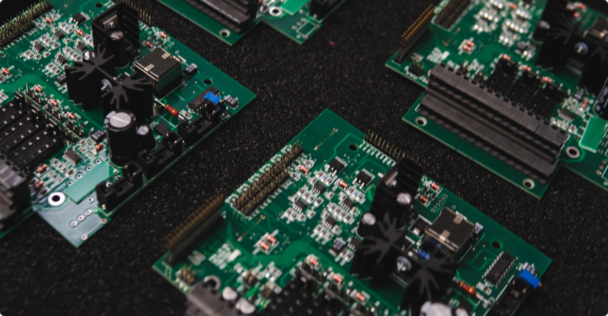
Printed circuit boards are a combination of so many elements, including the board itself, conductors, capacitors, diodes, transistors, etc. The board goes through different processes and PCB gold plating is one of them. In this process, the manufacturers apply a thin film of gold by using electroplating. They use nickel and gold alloy, in this case, as real gold is very soft. So, you can also call the process hard plating.
Advantages of PCB Gold Plating
Engineers use aPCB gold plating kit for surface treatment to avoid certain environmental conditions. Each PCB has a copper layer where you can apply nickel plating. After that, you can apply gold plating, making the board durable. Let’s look at the advantages of gold plating on circuit boards.
It Resists Corrosion: Gold does not cause any issues when exposed to oxygen, hence it prevents corrosion. It is better than copper or silver in terms of corrosion resistance. It is compatible with both industrial and natural environments.Gold-plated components don’t have to face frequent replacement so they increase a board’s life.
Good Conductor: Gold is ideal in terms of conductivity, be it heat or electricity. The thermal conductivity of gold is near 310 W m-1 K-1, whereas its electrical resistivity at 20 degrees centigrade is 0.022 micro ohm. Gold is a great conductor as its conductivity stays stable in different environments. Moreover, it provides a smooth surface and helps have a stable connection with the board.
Easy to Handle: According to experts, a thick layer of any metal can affect the performance of a circuit board. Gold is easy to develop into a thin layer for plating any PCB components. Moreover, thin coating can help you reduce the cost of plating.
Heat Resistant: PCB gold plating protects the components in hot environments. Gold can bear high heat as its melting point is high. It does not lose its properties in the high heat. Gold can protect electrical gadgets from any damage that may occur due to heat exposure.
Long-Lasting: Since gold does not corrode during wear and tear, it stays durable for a long time. In other words, gold plating makes a PCB long-lasting.
Less Degradation: Gold does not fret while interacting with other surfaces. So, it is not vulnerable to wear if there is any friction between gold and other metals or surfaces. Hence there is zero fretting corrosion.
However, to get all the above benefits, make sure that gold plating has enough thickness. Moreover, the process of gold plating PCB should be well- managed.
PCB Gold Plating Types
Different types of gold plating are in practice and engineers choose them according to the purpose of the board.
1-ENIG (Electroless Nickel Immersion Gold)Finish
PCB designers also call it soft gold plating. The thickness of the plate ranges between 1 and 3 micro inches. ENIG resists oxidation, and you can apply it evenly to get a flat surface. Such a smooth finish helps in assembling the fine-pitched components in SMD.
Some experts suggest the thickness of gold plating PCB from 4 to 8 micro inches, but it should be avoided. Additional thickness can harm nickel plating, besides it goes beyond the design standards. ENIG protects the nickel below, creating a smooth surface to solder.
2-ENEPIG (Electroless Nickel Electroless Palladium Immersion Gold) Finish
In ENEPIG, you will see palladium along with the same ENIG combination. Engineers use palladium to deal with black pads and non-wetting issues that happen in ENIG. However, this process increases the time and cost involved, depending on the production volume. However, it is durable and ideal for wire bonding.
3-PCB Gold Finger Plating
You must understand the PCB gold finger plating process. Gold fingers are columns that you can see on the PCB pads. It is hard gold plating on thePCB edge so you can also call it edge connector. You will see gold fingers in graphic cards, memory sticks, and other parts.
You can observe the graphic card slots in a computer PCB. These are PCB pads arranged as narrow rows on rectangular pads. Since the conductive pads resemble fingers, that’s why the name is so.Gold fingers are thicker than other PCB pads. Generally, the gold thickness in gold fingers is from 3u to 50u. In this case, the gold is an alloy which is harder than immersion gold.
Types Of Gold Fingers
There are three types of gold fingers as described below.
Traditional Gold Fingers for PCB
They are very common in practice having smooth array and level. The width, length, and clearance of PCB pads are similar.
Irregular Gold Fingers
In this case, PCB pad parameters vary. Like, they vary in length but have the same widths. Even the distance between fingers may vary in certain cases.
Segmented Fingers
In this case, the PCB pads vary in length. Besides there are segments of gold fingers.
Benefits of Gold Fingers in PCB
- The gold fingers are in direct contact with the PCB. Such a connection is highly conductive and mechanically durable compared to the PCB wires or conductors.
- They can bear any environmental wear and tear. Hence, you can plug in and out a PCB several times.
- High thickness of gold makes the PCB pads highly durable.
- Gold fingers can connect with the slots in different industrial and commercial devices. Similarly, engineers use gold fingers for interface connections in multiple systems.
- Since the process is hard, it makes gold plating resistant to oxidation.
Difference Between Immersion Gold and Hard Gold Plating
- Hard gold plating is a combination of nickel and gold that go through electroplating. In immersion gold, the manufacturer put a layer of gold on the copper through a chemical without using any electroplating.
- The EMIG process comes after soldering,but you have to do hard gold plating before soldering in PCB.
- Immersion gold is yellower than hard gold having the same thickness.
- As compared to immersion gold, hard gold plating provides a better connection and wear resistance.
Gold Finger Plating Process In PCB Manufacturing-Hard Plating
The PCB gold finger plating process provides a hard finish. It involves hard electroplating of gold where gold is electroplated on the PCB pads.
Let’s explore the different steps involved in the PCB gold finger plating process.
First Step: First, the PCB assemblers apply blue glue on the areas without gold fingers or hard plating. It makes the conductive angle parallel to the board direction without any issue.
Second Step: This step involves the oxidation removal from the copper surface. It is easy to do by using sulfuric acid that removes the oxidation. Later, you can clean that area with water. Then sandpaper the pad area and clean it with normal and deionized water.
Third Step: Now comes the electroplating of nickel on the PCB pads. After that, you have to wash away the debris with deionized water and normal water.
Fourth Step: Now, you have to apply a gold film on the nickel film on the PCB pads. Here again, you have to wash away unwanted particles or debris from the gold fingers.
Fifth Step: After hard plating your PCB, you have to remove the blue glue. After that comes the rest of manufacturing, including soldering and printing.
Though the PCB gold finger plating process is simple, a few manufacturers practice it. The processinvolves certain challenges, such as;
- The gold used in hard plating has a toxic salt named potassium cyanide. So, only limited PCB companies have permission to buy that salt.
- You should design a special system to get rid of wastewater or chemicals discharged during the process. You need a special license to provide such a finish.
Bevel Angle for PCB Gold Fingers
You need to provide a certain angle in the gold finger plating. The bevel angle, in this case, is often 45 degrees, depending on the PCB function. However, the angle can also be 20 or 30 degrees.
It is easy to bevel the gold finger with a machine to cut the PCB edge. Generally,assemblers use automatic technology in this regard. Beveling with a machine becomes essential when the gold fingers vary in direction. The cutting equipment is either fully automatic, or half automatic.
Final Thoughts
In PCB gold plating,manufacturers apply a thin film of gold by using electroplating. You have to use nickel and gold alloy, in this case, as real gold is very soft. Engineers also call the process hard plating.Such a surface treatment helps avoid certain environmental conditions. Each PCB has a copper layer where you can apply nickel plating. After that, you can apply gold plating, making the board durable.
There is also soft gold plating known as ENIG and ENEPIG of which the latter is time-consuming and costly. Hard gold plating is also known as gold finger plating.Gold fingers are columns on the PCB pads. Hard gold plating lies on the PCB edge, so you can also call it the edge connector. You will see gold fingers in graphic cards, memory sticks, and other parts.
Understanding ENIG
ENIG is an abbreviation of electroless nickel immersion gold. As the name shows there are two finishing layers, including nickel and gold. First, you immerse copper pads in nickel and then in gold salt with the help of a replacement reaction. PCB manufacturers apply ENIG on selective pads, and the rest of the pads can be finished with HASL, OSP, immersion tin, etc.
Positive Aspects of ENIG
- It has great wear resistance.
- It provides a smooth finish for a ball-grid array or in tiny components.
- It is ideal for electrical inspection points in the PCB.
- It is compatible with a wire bonding and an edge-card connector.
- ENIG is a cost-effective finish.
Negative Aspects of ENIG
- Black pads may occur during the process of ENIG due to irregular nickel and gold processes.
- PCB finish can be affected due to the thickness of gold and nickel.
ENIG has a low wet factor.
ENEPIG Vs ENIG
When it comes to ENEPIG Vs ENIG, you will see that ENIG is ideal for low-end products. ENEPIG is better in solderability and wire bonding than ENIG, besides ENIG is selective but ENEPIG is non-selective. Since ENEPIG is expensive due to gold and palladium, so ENIG is a better option for low-budget and selective projects.
Note: The thickness of the layers varies in both ENIG and ENEPIG.
Copper Core in PCB
Early PCBs used to be of paper and resin, but later on, more compact PCBs evolved due to compact devices. Traditional boards were without any insulation which is now common in the form of copper PCB. Designers introduced copper to create boards with more thermal conductivity.
Many electronic devices emit heat, hence a copper core PCB becomes a thermal conductor, sending the heat somewhere else. Copper protects the sensitive parts of the board from getting overheated.
Another quality of copper is that it enhances a board’s mechanical strength. Such a quality protects a device facing any physical stress. Copper adds life to the board, making it long-lasting.
A copper core PCB is a combination of copper, insulation, and copper substrate. It is also known as a copper-based circuit board, or a copper-clad, or a copper- substrate printed circuit board. It is ideal for the LED industry and it consists of four types, such as:
- Copper core PCB with a normal stack.
- Chip-on-board copper circuit board
- Aluminum-copper PCB
- Copper-core board with a direct thermal route
ENIG Vs HASL
Both ENIG and HASL are PCB finishes.
HASL (hot air solder leveling) is a surface finish for circuit boards. In this process, the manufacturer puts a PCB in a hot bath of solder and levels it with hot air. Whereas in ENIG, a layer of electroless nickel and gold is applied to the board surface.
HASL is cost-effective, easy to work with, and it is always available. However, it is thicker compared to ENIG, so you cannot use it for SMD components.
On the other hand, ENIG is ideal for intense environments and is more reliable. It is ideal for military, aerospace, medical, and marine industries. However, ENIG is costly compared to HASL.
YOU MIGHT ALSO LIKE
Share: