
Unlocking Efficiency with IC Decapsulation in Printed Circuit Boards

Admin, February 01,2024
PCBA Manufacturing Processes and Technologies
PCBA Manufacturing Processes and Technologies
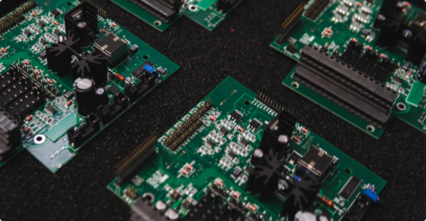
The printed circuit board sends the current through copper routes to help an electronic device function. Engineers have to install the required components on a bare PCB for current flow and that process is known as PCB assembly. Here, we will discuss various steps of PCBA manufacturing. You cannot complete the assembly process by missing any step in this regard.
However, the process also depends on the nature of the assembly as it has different types such as,
- Single-sided PCBA
- Double-sided PCBA
- Mixed single-sided having SMD and THC
- One side with SMD and THC, and another side with THC only.
- One side has SMD, and the other has THC.
Let’s discuss the PCBA In general.
Applying The Solder Paste
Soldering is a process of connecting two components on a printed circuit board. First, you need a stencil that can help you to apply the solder paste in the required areas. There are two types of stencils in this case, including stencil printers and laser-cut. The latter is more precise involving fewer errors.
Component Arrangement
Now, you can place the components on the soldered areas according to the design. Make sure that components and solder paste are aligned, or they will lead to a faulty PCB. Manufactures perform this step in different ways, such as:
Using Automated Tools: It involves machines having empty nozzles to pick and place the components on the required spots. Advanced machines are robotic and work very fast as they can perfectly arrange thousands of parts in an hour.
Using Feeders: This technique involves feeders to supply the components to the machine. The feeders vary according to the components like the tray feeders help in bulk components, reel feeders are ideal for tape and reel components, whereas ICs need tube feeders.
Using Cameras: It involves machines having cameras to monitor the exact placement of very delicate and small components. The machines work through specific design parameters provided by design software. The software data optimizes the entire process and reduces the job time. Similarly, PCBA Manufacturing involves quality control to check the placement of the components. The best PCB manufacturing companies use special systems to monitor the process during component installment.
Joining the Components
Now comes the process of joining the components with the board through reflow soldering. The assembler put the board in the oven to heat the solder paste to create a solder joint. It sticks the component to the board. The oven provides heat according to the soldering component type. The reflow process involves 4 stages, such as:
Soaking: This is the preheating of the board before the solder paste’s melting stage. It slowly heats the circuit board to avoid component displacement, evaporating extra solvents.
Temperature Control: Reflow soldering involves a thermal profile to manage heat. It is an essential factor to ensure precise soldering and fewer errors. Moreover, the profile reduces thermal stress which can damage the components.
The Reflow: Now comes the reflow process where the temperature has to be more than the melting level of the solder. This process melts the solder, bonding the components on the circuit board. You will get a durable joint through surface tension that occurs through melting. The reflow keeps the components intact, and eventually, you get long-lasting PCBA manufacturing.
The Cooling Process: Now comes solder cooling that hardens the joints. However, you need balanced cooling to avoid thermal shocks. Cooling helps have powerful solders with excellent electrical and mechanical strengths.
Inspection: After fixing the components through soldering, manufacturers perform AOI to test the quality of the assembly. The automatic optical inspection involves a camera to find the surface flaws. Another method to do so is an X-ray to check the solder joints. Another technique is 3D SPI to measure the volume and application of the solder paste.
Through-Hole Mounting
Some PCBAs involve the through-hole technique. It consists of a machine that provides wave or selective soldering, depending on the nature of the project.
Final Testing
The final PCBA manufacturing testing can be ICT or in-circuit testing to check the current flow passing through the routes. Likewise, the testing rigs check the overall environment to see if the PCB functions well.
Chemical Coating
In certain cases, manufacturers protect the final circuit board through chemical coating. It helps to protect the board from rain, dust, cold, heat, and other environmental issues. You can apply it through the spray and then cure it with UV rays. You can also manually apply the chemical coating with a brush. Another way is to dip the circuit board in the chemical as in mass production. Sometimes coating involves a machine to cover certain areas, preventing heat sinks.
The coating materials, in this case, can be any including, acrylic, epoxy, silicone, urethane, or perylene. Each material has its properties and you can use them according to the environment where that PCB will be used. Like, urethane is suitable for chemical-rich environments whereas acrylic provides basic protection. Silicon is suitable for hot areas, whereas epoxy is not ideal when you need to rework as you cannot remove it easily. After all the above steps, PCBA should go into packaging for shipping. Make sure it is highly safe.
Copper Trace In PCB - The Movement Of Current In Components
PCB assembly involves the arrangement of components and placing them through soldering. Electrical components carry the current but do you know how this current moves between the components?
PCB has a thin film of copper known as a copper trace that helps move the current between the components. Circuit boards cannot carry the current without copper traces, as they won’t function.
Manufacturers etch the board surface with copper that we call tracks or traces. In other words, it works like a copper wire without insulation. However, copper trace is a flat film of copper.
Copper strips or traces help PCB components connect, passing the current between these components. You have to determine the trace thickness according to the current it has to carry. Engineers design thick traces for more current whereas thin traces are ideal in situations where you need less current.
Important Elements of Copper Traces
There are many benefits of using copper in a PCB, such as:
According to experts, copper is an excellent conductor, hence ideal in current transmission. So, there are fewer chances of heat loss and resistance.
Copper is ani-rust and does not wear so that increases its life. Such a durable metal is ideal for devices that work in unsuitable environments.
When it comes to flexibility, copper trace is at the top. You can twist copper as you want according to the design of the circuit board. That’s why most devices come up with copper traces on their circuit boards.
Copper Power Calculator-Additional Info
PCB designers have to follow certain design parameters to ensure a good flow of current through the components. As you know, copper is an essential element in the circuit board so finding its power is crucial for a good PCB. Engineers use a copper power calculator to evaluate the heat, power loss, and effectiveness of copper. So, the calculation helps designers in designing a reliable device.
The calculation involves certain formulas based on the symbols depicting the power loss, resistance, and current, such as:
P=I2R
The above equation can help you to find the heat dissipated by a copper conductor that happens due to resistance. P stands for power loss measured in watts, whereas I is the current measured in amperes and R or resistance is measured in ohms.
Remember to use the calculator in a systematic way. Like, finding the flow of current in copper conductors, as well as resistance. Then put all these values into the above formula and get the results.
The copper power calculator helps determine the size of the conductor to carry the balanced amount of current. Large conductors are less prone to heat loss and don’t resist much. This way, you can protect an electrical system from any damage.
Evaluating the Copper Width
The calculator helps evaluate the width of copper for which you need its properties, current, and temperature. So, you can easily find the trace size for your PCB.
How to Calculate the Copper Trace Resistance
You can find the resistance of copper trace through its width, length, and temperature. The outcome will help you find the resistance that you have to face while designing the copper trace.
Final Thoughts
When it comes to PCBA manufacturing, make sure every step goes well to ensure an effective product. Soldering is a process of connecting two components on a printed circuit board. You need a stencil to help you apply the solder paste in the required areas. New technology, inspection techniques, and advanced automation keep on enhancing the process of PCBA. There are different ways to assemble a circuit board, and you can choose the one according to your project. You can also use a calculator to find the copper power. Moreover, the manufacturer should have a good knowledge of all the steps involved in PCB assembly.
YOU MIGHT ALSO LIKE
Share: