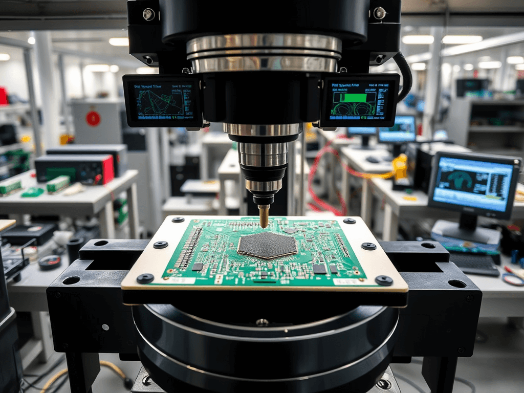
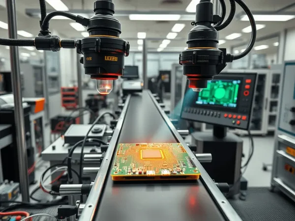
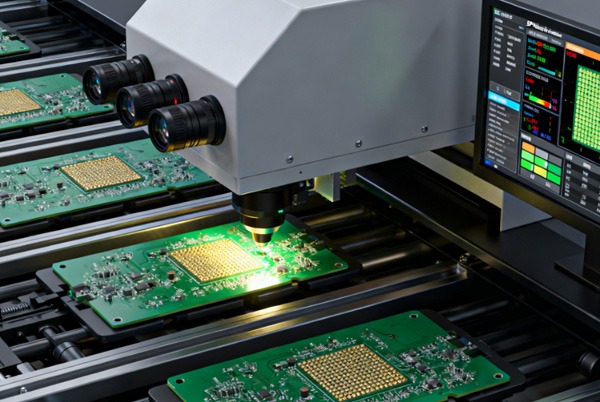
Solder paste inspection (SPI) is a critical quality control step in surface-mount technology (SMT) electronics manufacturing that uses 3D scanning or optical imaging to verify that solder paste is applied correctly before components are placed
2 KOH YOUNG:2 KOH YOUNG Solder Paste Inspection Machines Ensures the accurate deposition of solder paste by detecting misalignment, insufficient paste, or excessive deposits early in the process.
solder defects:Prevent defects like solder bridges or open circuits, reducing rework and scrap rates.
SPI :SPI improves production quality, enhances process control, and ensures consistent solder joint reliability, ultimately saving time and costs in high-volume manufacturing.
High-Precision 3D Solder Paste Inspection – Accurately measures solder paste volume, height, area, and alignment to ensure consistent deposition before component placement.
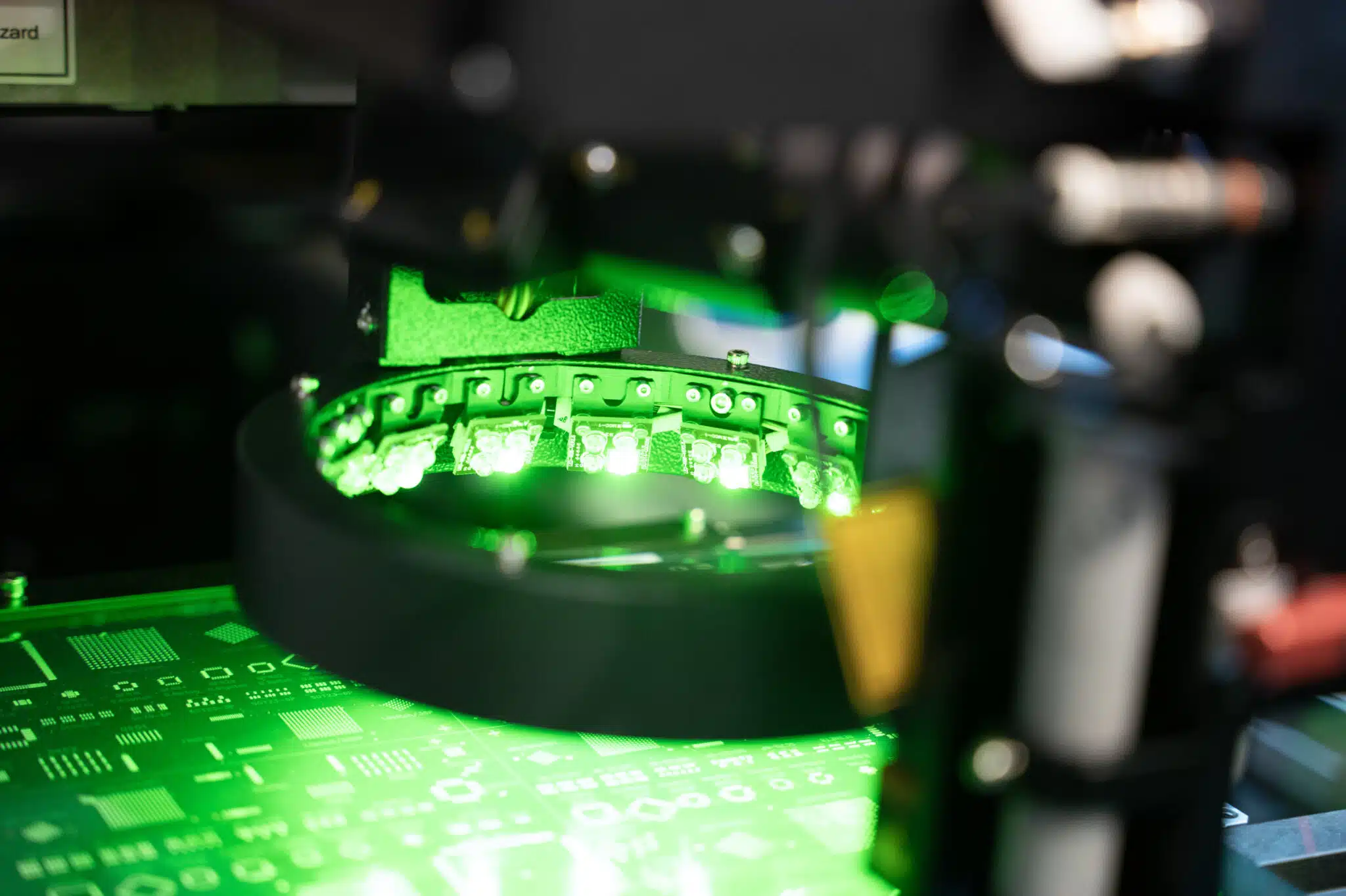
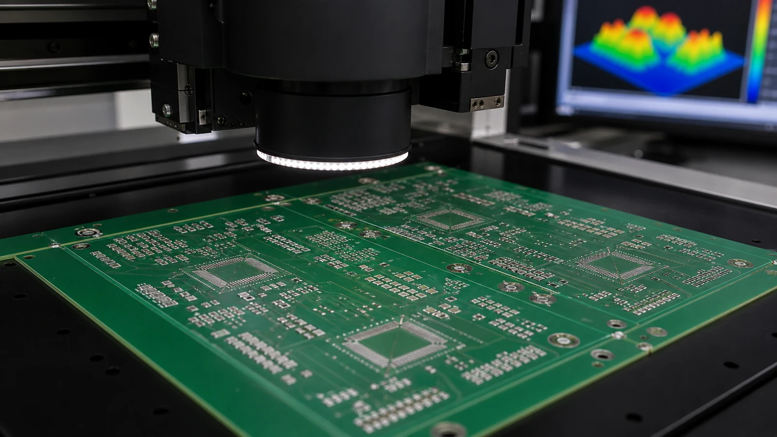
At Altest Corporation, our Solder Paste Inspection (SPI) process ensures the highest level of accuracy during Surface Mount Technology (SMT) assembly by verifying solder paste deposits before component placement. As the first quality gate in the SMT production process, SPI plays a critical role in detecting printing defects that can lead to solder joint failures, rework, and reduced manufacturing yields. Using advanced 3D SPI inspection systems, we accurately measure solder paste volume, height, area, shape, and alignment, ensuring every PCB is prepared for reliable component placement and reflow soldering.
Our automated SPI systems utilize high-resolution 3D optical imaging technology to inspect every solder paste deposit with exceptional precision. The system identifies common printing defects such as insufficient solder paste, excessive paste volume, bridging, smearing, stencil misalignment, missing deposits, offset printing, and solder contamination before components are mounted. Real-time process monitoring enables our manufacturing engineers to optimize stencil printing parameters, improve process stability, and maintain consistent quality across prototype, low-volume, and high-volume production.
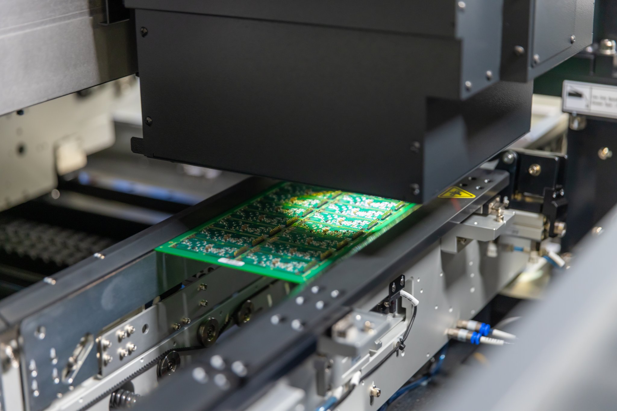
With decades of expertise in PCB assembly and Electronics Manufacturing Services (EMS), Altest Corporation combines advanced inspection technologies with rigorous quality assurance to deliver consistently reliable SMT production. Our investment in cutting-edge 3D SPI equipment, experienced process engineers, and data-driven manufacturing enables us to achieve superior process control, reduce production costs, and deliver high-quality PCB assemblies for industries including aerospace, defense, medical, automotive, telecommunications, industrial automation, and consumer electronics.
Find answers to common questions about 3D Solder Paste Inspection, closed-loop feedback, defect prevention, and volumetric measurement.
SPI, or Solder Paste Inspection, is an automated quality assurance process performed immediately after the solder paste is printed onto the bare circuit board. It uses specialized cameras and lighting to measure the exact amount of wet paste deposited on every single pad before any electronic components are placed.
Industry data proves that over 70% of all surface mount defects—such as solder shorts, bridging, open joints, and tombstoning—are directly caused by improper solder paste printing. SPI catches these errors at the very beginning of the line, drastically reducing the need for expensive and time-consuming rework after the board has gone through the reflow oven.
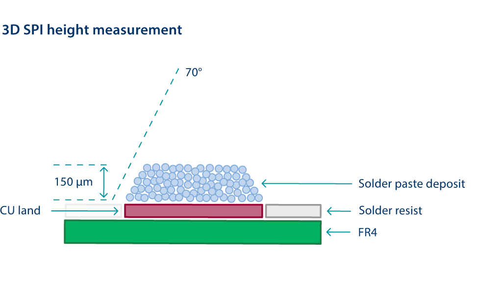
2D SPI only measures the surface area and X/Y positional offset of the paste. It cannot tell how thick the paste is. 3D SPI, which we use exclusively, utilizes phase-shift profilometry (lasers and structured light) to create a topographical map of the paste. This allows us to calculate the exact height and true volumetric mass of the deposit, which is critical for component reliability.
Our 3D SPI systems evaluate every single pad for five primary parameters: Paste Volume (is there enough solder?), Height (is the stencil lifting cleanly?), Area (is the spread correct?), Positional Offset (is the paste perfectly aligned with the copper pad?), and Bridging (is paste bleeding between two adjacent pads?).
If a board violates any programmed tolerance, the SPI machine halts the line and sounds an alarm. Because the board has not yet received components or been baked, recovering it is simple. The operator simply removes the board, wipes away the wet paste using an ultrasonic solvent cleaner, dries it, and sends the bare board back to the printer for a fresh run.
Yes. Our high-resolution SPI cameras are specifically calibrated to inspect extremely dense High-Density Interconnect (HDI) boards. They can accurately measure paste deposits for microscopic 01005 discrete components and ultra-fine pitch BGAs down to 0.3mm spacing with sub-micron height resolution.
Closed-loop feedback is an advanced Industry 4.0 feature where the SPI machine communicates directly with the solder paste printer. If the SPI detects a trending drift in paste alignment or volume over several boards, it automatically sends algorithmic offset corrections to the printer to fix the issue before a failing board is ever produced.
No. Modern inline 3D SPI machines are incredibly fast. They utilize high-speed imaging "on the fly" without having to stop the camera head for every component. This ensures the SPI cycle time is equal to or faster than the screen printer and pick-and-place machines, causing zero bottlenecks.
For all IPC Class II, Class III, medical, and aerospace assemblies, we mandate 100% inline SPI inspection. Every single pad on every single board is mathematically verified to ensure absolute zero-defect reliability before it moves to component placement.
Yes. The SPI system generates a comprehensive statistical report (Cpk, gauge R&R) and saves a 3D topographic image of the solder deposits for every board run. This data is linked to the board's serial number or barcode, providing complete manufacturing traceability for strict regulatory environments like FDA or ITAR compliance.
Partner with Altest Corporation for your next high-reliability PCB fabrication and turnkey SMT assembly project. Our engineering team is ready to review your gerber files and provide a detailed, competitive estimate.

